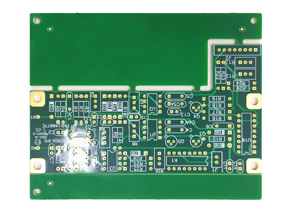
HDI PCB Multilayer Fr4 Printed Circuit Board Blind Buried Holes Immersion Gold
Technical & Capability
| Item | Production Capacity |
| Layer Counts | 1-20 layers |
| Material | FR-4,Cu base,High TG FR-4,PTFE,Rogers,TEFLON etc. |
| Board thickness | 0.20mm-8.00mm |
| Maximum Size | 600mmX1200mm |
| Board Outline Tolerance | +0.10mm |
| Thickness Tolerance(t≥0.8mm) | ±8% |
| Thickness Tolerance(t<0.8mm) | ±10% |
| Insulation Layer Thickness | 0.075mm--5.00mm |
| Minimum Line | 0.075mm |
| Minimum Space | 0.075mm |
| Out Layer Copper Thickness | 18um--350um |
| Inner Layer Copper Thickness | 17um--175um |
| Drilling Hole(Mechanical) | 0.15mm--6.35mm |
| Finish Hole(Mechanical) | 0.10mm-6.30mm |
| Diameter Tolerance(Mechanical) | 0.05mm |
| Registration(Mechanical) | 0.075mm |
| Aspect Ratio | 16:1 |
| Solder Mask Type | LPI |
| SMT Mini.Solder Mask Width | 0.075mm |
| Mini. Solder Mask Clearance | 0.05mm |
| Plug Hole Diameter | 0.25mm--0.60mm |
| Impedance control Tolerance | ±10% |
| Surface finish/treatment | HASL,ENIG,Chem,Tin,Flash Gold, OSP, Gold Finger |
PCB advantages:
1 R&D team support
2 UL, RoHS,ISO9001,SGS
3.IPC class2
4.Advanced production line and promtly delivery.
5. Honest Credibility in China.
6. Professional and abundant experience in PCB.
7. Competitive price and good quality.
8. Excellent after-sales service.
| Production capacity of hot-sale products |
| Double Side/Multilayer PCB Workshop | Aluminum PCB Workshop |
| Technical Capability | Technical Capability |
| Raw materials: CEM-1, CEM-3, FR-4(High TG), Rogers, TELFON | Raw materials: Alurminum base, Copper base |
| Layer: 1 layer to 20 Layers | Layer: 1 layer and 2 Layers |
| Min.line width/space: 3mil/3mil(0.075mm/0.075mm) | Min.line width/space: 4mil/4mil(0.1mm/0.1mm) |
| Min.Hole size: 0.1mm(dirilling hole) | Min.Hole size: 12mil(0.3mm) |
| Max. Board size: 1200mm* 600mm | Max.Board size: 1200mm* 560mm(47in* 22in) |
| Finished board thickness: 0.2mm- 6.0mm | Finished board thickness: 0.3~ 5mm |
| Copper foil thickness: 18um~280um(0.5oz~8oz) | Copper foil thickness: 35um~210um(1oz~6oz) |
| NPTH Hole Tolerance: +/-0.075mm, PTH hole Tolerance: +/-0.05mm | Hole position tolerance: +/-0.05mm |
| Outline Tolerance: +/-0.13mm | Routing outline tolerance: +/ 0.15mm; punching outline tolerance:+/ 0.1mm |
| Surface finished: Lead free HASL, immersion gold(ENIG), immersion silver, OSP, gold plating, gold finger, Carbon INK. | Surface finished: Lead free HASL, immersion gold(ENIG), immersion silver, OSP etc |
| Impedance control tolerance: +/-10% | Remain thickness tolerance: +/-0.1mm |
| Production capability: 50,000 s.q.m/month | MC PCB Production capability: 10,000 s.q.m/month |
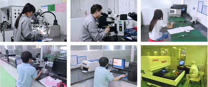
Quality Control:
All department implements according to ISO and the related dept has to provide 8D report if any board scrapped to defective.
All the outgoing boards have to be 100% electronic tested, impedance tested and soldering.
Visual inspected, we make the inspect microsection before shipment.
Train the mindset of employees and our enterprise culture, make they happy with their work and our company, it's helpful for them to produce good quality products.
High quality raw material (Shengyi FR4, ITEQ, Taiyo Solder Mask Ink etc.)
The AOI could inspect the whole set, boards are inspected after each process
Company:
Abis Circuits C o., Ltd Created in 2006,as a long history China based PCB supplier, ABIS manufactures different kinds of printed circuit boards, including MCPCB,CEM-1,CEM-3,and FR4,FR-4 high Tg, Rogers, Teflon, Arlon ets special material.
ABIS has set up two PCB factories in China: one for MCPCB producing, quick turn and small volumn making, and another for mass production. Currently, ABIS modern plants occupy total 10000 s.q.m facility, with more than 1100 stable and experienced workers. Professionalism and continuous optimization of manufacturing processes have positioned ABIS as a reliable and favorite partner for global companies
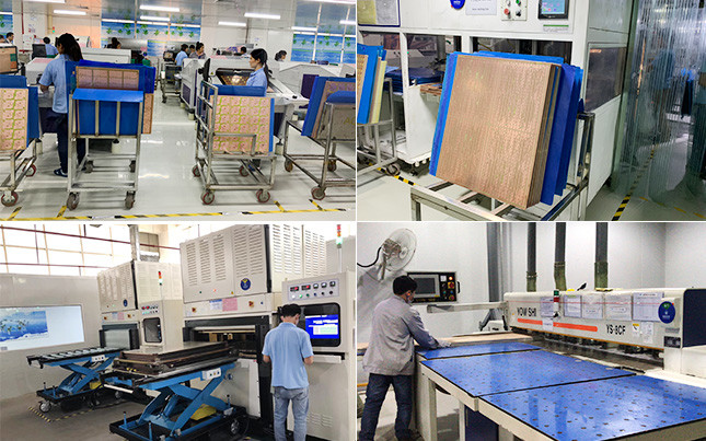
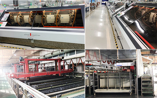
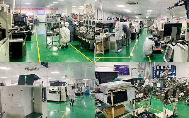
Workshop:
FAQ:
Q1:What's your Aluminum board Thermal Conductivity?
A: Normally 0.8-3W/m.K. If you have special demands please feel free contact us.
Q2:Is my PCB file safe if I send it to you for manufacturing?
A: We respect customer's design authority and will never manufacture PCB for someone else without your permission. NDA is acceptable.
Q3:What is your testing policy and how you control the quality?
A: For sample, usually tested by flying probe; for PCB Volume over 3 square meters, usually tested by fixture, this will be more faster.
Due to there's many steps to PCB production, we usually do inspection after every step.
Q4: What's your shipping way ?
A: 1. We have our own forwarder to ship goods by DHL, UPS, FEDEX, TNT,EMS.
2. If you have your own forwarder, we can cooperate with them.
Q5: What is your certificate?
A: ISO9001:2008, ISO14001: 2004, UL, SGS,RoHS report.
Q6: What files should we offer?
A: If only need PCB, please provide Gerber File and manufacturing specifications; If need PCBA,Please provide Gerber File,
Manufacturing specification, BOM list and Pick & Place/XY file.
Q7: Can I get a sample?
A: Yes, It's reasonable to get a sample to test our quality at first.
Q8: Why choose us?
A: With ABIS, customers significantly and effectively reduce their global procurement costs. Behind each service provided by ABIS,
is hidden a cost saving for customers.
Product Tags:

|
|
Multilayer OSP 175um Fr4 HDI PCB Board Blind Buried Holes HASL LPI Images
|