HDI Multilayer Green Ink Printed Circuit Board 10L PCB Prototype Hidh Speed For Electronic
Company Profile
Abis Circuits Co., Ltd is a professional PCB manufacturer which was established on Oct, 2006 and focus on double side, Multilayer and HDI PCB mass production. We have two factories together , the factory in Shenzhen is specialized in small and middle volume orders and the factory in Jiangxi province is for big volume and HDI. Our aim is help the clients gain more competitive strength and bring more mutual benefit to each other. All clients will be served well.
About Quotation: 1 Hour quotation
2 hours complain feedback
7*24 hour technical support
What is a HDI PCB?
IPC-2226 defines HDI as a printed circuit board with a higher wiring density per unit area than conventional printed circuit boards (PCB). They have finer lines and spaces ≤ 100 µm / 0.10mm, smaller vias (<150 µm) and capture pads <400 µm / 0.40mm, and higher connection pad density (>20 pads/cm2) than employed in conventional PCB technology.
Product Detail
1. Rigid, Flex, Rigid-Flexible PCB.
2. Buried/Blind Vias, Via in Pad, Counter Sink Hole, Screw Hole(Counterbore), Press-fit, Half Hole.
3. HASL lead-free, Immersion Gold/ Silver/Tin, OSP, Gold plating/finger, Peelable mask,
4. Printed Circuit Boards adhere to IPC Class 2 & 3 international PCB standard.
5. Quantities range from prototype to medium & big batch production.
Product Description
| Item | Spec |
| Layers | 1~20 |
| Board Thickness | 0.1mm-8.0mm |
| Material | FR-4, CEM-1/CEM-3, PI, High Tg, Rogers, PTEF, Alu/Cu Base, etc |
| Max Panel Size | 600mm×1200mm |
| Min Hole Size | 0.1mm |
| Min Line Width/Space | 3mil(0.075mm) |
| Board Outline Tolerance | 士0.10mm |
| Insulation Layer Thickness | 0.075mm--5.00mm |
| Out Layer Copper Thickness | 18um--350um |
| Drilling Hole (Mechanical) | 17um--175um |
| Finish Hole (Mechanical) | 0.10mm--6.30mm |
| Diameter Tolerance (Mechanical) | 0.05mm |
| Registration (Mechanical) | 0.075mm |
| Aspect Ratio | 16:01 |
| Solder Mask Type | LPI |
| SMT Mini. Solder Mask Width | 0.075mm |
| Mini. Solder Mask Clearance | 0.05mm |
| Plug Hole Diameter | 0.25mm--0.60mm |
| Impedance Control Tolerance | 士10% |
| Surface finish | ENIG, OSP, HASL, Chem. Tin/Sn, Flash Gold |
| Soldermask | Green/Yellow/Black/White/Red/Blue |
| Silkscreen | Red/Yellow/Black/White |
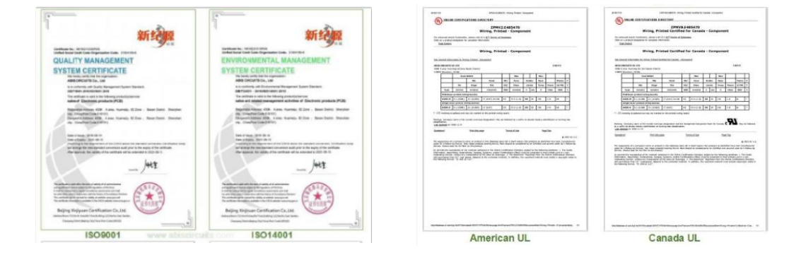
| Certificate | UL, ISO 9001, ISO14001, IATF16949 |
| Special Request | Blind hole, Gold finger, BGA, Carbon ink, peekable mask, VIP process, Edge plating, Half holes |
| Material Suppilers | Shengyi, ITEQ, Taiyo, etc. |
| Common Package | Vacuum+Carton |
Capacity
| Max. No. of Layers | 20 |
| Max. Board Size | 860*610mm |
| Board Thickness | 0.2-6.0mm |
| Copper Thickness | 0.5OZ-6OZ |
| Material | Various |
| Surface Finish | Various |
| Soldermask | Various |
| Minimum Soldermask Thickness | 0.025mm |
| Minimun Soldermask BridgeDam | 0.15mm |
| Minimum Soldermask Clearance | 0.075mm |
| Peelable Colours | Blue |
| Peelable Minimum Feature | 0.5mm |
| Peelable Maximum Tented Hole | 3.0mm |
| Scoring Angle | 30 Degrees |
| Min. Remaining Thickness | 0.3mm |
| Min. Distance to copper (From center of scoring line) | 0.5mm |
| Min. Track | 0.1mm |
| Min.Gap(TrackTrack,TrackPad,PadPad) | 0.1mm |
| NPTH Min. Drill Size | 0.2mm |
| Plated Drill Size | ± 0.075mm |
| Non-Plated Drill Size | ± 0.05mm |
| Drill Location Tolerance | ± 0.05mm |
| OutlineRouted Slots | ± 0.1mm |
| Line Width/Spacing | ±10% |
| Board Thickness | ±10% |
| Warp and Twist | 0.05% |
| Scoring/V-Cut | ± 5 degrees |
| Scoring Positional Tolerance | ± 0.1mm |
| Aspect Ratio | 10:01 |
Lead Time
| Number of Layers | Quick Turn Lead Time |
| 2 | 24 Hours |
| 4 | 48 Hours |
| 6 | 72 Hours |
| 8 | 96 Hours |
| 10 | 120 Hours |
| 12 | 120 Hours |
| 14 | 144 Hours |
| 16 | Depend on Technical Specification |
| 18 | Depend on Technical Specification |
| 20 | Depend on Technical Specification |
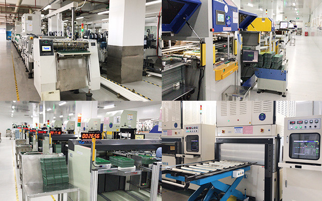
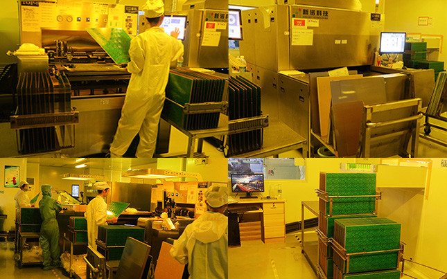
Work Shop
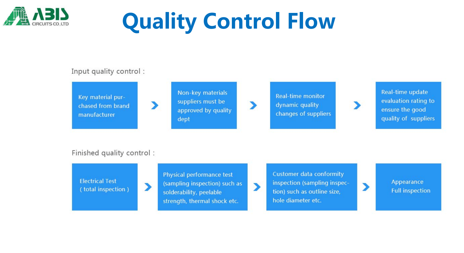
Quality Control
Certificate
FAQ
Q1:When can I get the quotation?
A:We usually quote with 1 hour after we get your inquiry. If you are very urgent, please call us or tell us in your email.
Q2:I am a small wholesaler, do you accept small order?
A:It's no problem. If you're small wholesaler, we would like to grow up with you together.
Q3:How many days will samples be finished? And how about the mass production?
A:Generally 2-3 days for samples making. The lead time of mass production will depend on the order quantity and the season you place the order.
Q4:If I order big quantity, what's the good price?
A: Please send the details enquiry to us, such as the Item Number, Quantity for each item, Quality request, Logo, Payment Terms, Transport method, Discharge place etc. We will make the accurate quotation to you as soon as possible.
Q5:Can I have samples to test?
A: Yes, we are pleased to supply module samples to test and check quality, mixed sample order is available. Please note buyer should pay for shipping cost.
Q6:If all pcb , PCBAs will be tested before delivery if we provide the function testing method?
A:Yes, we ensure that each piece of pcb, PCBA will be tested before shipment, we ensure the goods we sent with good quality
Q7:What is the shipping method?
A:We suggest you using DHL, UPS, FedEX, TNT forwarder.
Q8:How about the payment terms?
A:By T/T, Paypal, Western Union, etc.
Why choose us?
·With ABIS, customers significantly and effectively reduce their global procurement costs. Behind each service provided by ABIS, is hidden a cost saving for customers.
. We have two shop together, one is for prototype, quick turn, small volume making. The other is for mass production also for HDI board, with highly skilled professional employees, for high quality products with competitive price and on-time delivery.
. We provide very professional sales, technical and logistic supports, on a world-wide basis.hours complaint feedback.
ABIS cares every your order even 1 piece
Product Tags:

|
|
PTEF 350um Multilayer HDI PCB Board ENIG 10L PCB Prototype Board For Electronic Images
|